Building photonic inference hardware in Boulder
Great Sky was founded in 2023 by researchers who spent a decade studying optical computing in national laboratories and university photonics groups. The company is focused on one problem: making neural-network inference cheaper to run at data-center scale by moving matrix computation out of transistor logic and into coherent light.
Why photonics, why now
The founding team spent years watching the gap between GPU inference efficiency and the theoretical efficiency of optical matrix computation grow wider. Academic results from MIT, Stanford, and NIST had demonstrated MZI mesh multiplication with energy costs orders of magnitude below digital CMOS. The gap between those results and a shipping product was not a physics problem; it was an engineering one: thermal stability, packaging integration, and a software layer that worked with existing inference frameworks.
In 2023 we decided to close that gap. We chose Boulder, Colorado because it puts us within one hour of several photonics research groups at NIST, CU Boulder, and Colorado State who have decades of device-level photonic expertise. We can move from a waveguide design question to a fabrication consultation without getting on a plane.
Our first full-wafer silicon photonic run taped out on the AIM Photonics multi-project wafer shuttle in late 2024. First silicon came back showing phase-setting accuracy within 0.03 radians of target across the full 512-element mesh, which was sufficient to begin characterizing matrix-vector multiplication fidelity at 8-bit effective precision. The evaluation program for qualified inference teams follows from those results.
Great Sky is angel-backed and operating on internal capital. We are not announcing funding; this page reflects the company as it stands.
The people building GSK-1
Three people with backgrounds in silicon photonics device physics, photonic chip architecture, and optical neural-network theory.
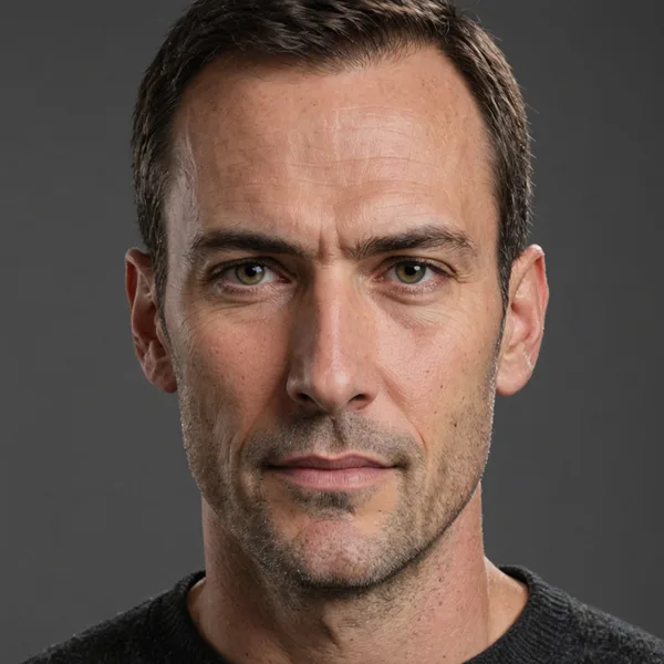
Jeff spent eight years as a research physicist at NIST Boulder studying superconducting photonic devices and optical computing architectures. He holds a PhD in physics from the University of Colorado. He leads product vision, hardware architecture, and investor relations.

Soren leads chip architecture and photonic device design at Great Sky. He holds a PhD in electrical engineering from KTH Royal Institute of Technology in Stockholm, and previously worked on waveguide layout and modulator optimization at two silicon photonic ASIC firms before co-founding Great Sky in 2023.

Yuna leads Great Sky's research program on optical neural-network architectures and inference precision theory. Her PhD at the University of Tokyo examined phase noise propagation in MZI mesh computing, and she bridges the academic photonic computing literature with the engineering constraints of the GSK-1 production design.
Boulder, Colorado
Our office and lab are at 1050 Walnut Street, Suite 300, Boulder CO 80302. We have a small photonics characterization lab on-site for device testing and evaluation kit preparation. Visitors are welcome by appointment.
For research inquiries and evaluation kit requests: [email protected]
Boulder is one of a small number of places in the US with a density of photonic device expertise outside of the major coastal tech hubs. NIST's Physical Measurement Laboratory, the CU Boulder photonics program, and the Colorado Photonics Industry Association are all within a short radius. That proximity shapes how we work.
+1 (303) 442-0175
1050 Walnut St, Ste 300
Boulder CO 80302